

Scanning Probe Microscopy Lab (SPMlab)
is a scanning probe microscopy (SPM) laboratory located at the Department of Physics of Nanostructures and Nanotechnology, Institute of Physics of the Jagiellonian University.
In the laboratory we conduct research focused on atomic and molecular structures constructed on crystalline surfaces. The techniques that we apply enable characterization of the analysed systems with sub-nanometer resolution. In other words, they allow us to see even single atoms.
Scanning Probe Microscopy
Scanning Probe Microscopy (SPM) can be treated as a group of research techniques derived from the two pioneering methods, i.e. scanning tunneling microscopy (STM) and atomic force microscopy (AFM), which dates back to the 1980s. Thus, they are relatively young research techniques, which in recent decades have certainly revolutionized the studies of surfaces, as well as the atomic and molecular systems constructed on them. The above-mentioned methods are based on the registration of electron tunneling between an atomically sharp tip and the tested objects (STM microscopy), or on the analysis of the forces acting between the tip and the surface nanostructures (AFM microscopy). The approach provides very local characterization and therefore is sensitive even to single atoms. In our laboratories, we perform measurements in ultra-high vacuum (UHV) conditions and at cryogenic temperatures to limit the impact of thermal excitations.
Research Areas
Atomic nanostructures on semiconductors
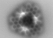
![Graphic showing a logic gate constructed on the Si (001):H surface [1].](/img/groups/spm/fig2.jpg)
One of the most interesting, though somewhat futuristic, concepts is the use of single organic molecules or atomic nanostructures playing an active role in future nanodevices. Therefore in our laboratories we construct atomic nanostructures on semiconductor germanium and/or silicon surfaces, quite naturally selected for electronics applications. These substrates could be regarded as the basic building materials in modern electronics, and in our experiments we passivate them with hydrogen. This provides decoupling of the on-surface created atomic nanostructures from the bulk crystal. In our research, we remove single hydrogen atoms one by one from the passivating layer and generate the nanostructures comprising the so-called surface dangling bonds, which are exposed after surface hydrogen atom removal. The objects of our interest are the electronic states located within the band gap of the substrate, provided by the above-described dangling bonds. By manipulating the exact location of the hydrogen vacancies, we can modify the coupling of the dangling bonds electronic states, and thus obtain various functionalities, e.g. logic gates [1]. The combination of the experimental techniques based on scanning tunneling spectroscopy with computational methods provides the approach for the design and construction of prototypical nanoscale circuitries, as well as the characterization of their transport properties [2].
Coupling organic molecules with single atoms on semiconductors
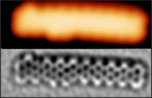
![Obraz STM molekuł starfen na powierzchni Ge(001):H [3].](/img/groups/spm/fig3.jpg)
The atomic nanostructures described in the previous section can be supplemented with organic molecules, and the dangling bonds allow to contact and couple the molecules with the substrate in a controlled manner [3]. This gives insight into the processes of chemical reactions and bond formation taking place between the molecules and the unpassivated semiconductor areas, usually present in the form of single atoms. This provides perspectives to enter the fascinating field of chemical engineering at the nanoscale. Interestingly, the interaction with the tip of the STM microscope makes feasible controlled breaking and restoring of chemical bonds, as well as the construction of nanoscale mechanical systems, e.g. molecular rotors, for which the hydrogen vacancies play a role of pivot points [4]. Thanks to the use of a unique multiprobe microscope, we can also control the transformations of the molecules in a remote manner.
On-surface synthesis of new molecules
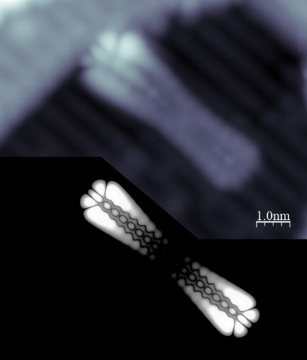
![Obraz 3D nc-AFM undekacena - acena zawierającego 11 pierścieni benzenowych [6].](/img/groups/spm/fig4.jpg)
The synthesis of molecular systems directly on surfaces is a relatively young, but dynamically developing area of research [5]. Initiated several years ago, it aims to create new molecular structures that could not be obtained with more traditional and otherwise fantastically developed methods of solution chemistry. An approach based on the so-called on-surface synthesis has brought a number of intriguing achievements in the last years allowing for the synthesis of molecular units with predicted interesting or exotic properties, that could not be generated even for decades. Among the most interesting new single molecules fabricated by the application of the surface assisted chemistry one can mention e.g. long acenes and their derivatives [6-9].
In general the most common approach for the synthesis of new single molecules is based on the preparation of special and stable molecular precursors, which on the surfaces undergo intramolecular transformations toward target objects. Of course, the key aspect here is the ability of atomically precise imaging, and therefore scanning probe microscopes play an important role. In particular, the key tool is the non-contact atomic force microscope with a functionalized tip (most often by a CO molecule) giving an unprecedented ability to provide bond-resolved images [10].
The importance of scanning tunneling spectroscopy, which enables an insight into the energies of electronic states and their spatial distribution, cannot be overlooked either. For several years, in cooperation with experienced teams synthesizing unique molecular precursors, we have been conducting experiments focused on acenes [6-7] and their derivatives [8, 9], as well as on various types of nanographenes [11-12]. Recently one of the most important and promising directions of our experiments is the transfer of the “on-surface synthesis” concepts onto the non-metallic, semiconducting or insulating, technologically relevant substrates [13-14].
Graphene nanoribbons (GNRs)
In addition to the synthesis of single molecules, based in principle on intramolecular transformations and presented in the previous section, the on-surface synthesis approach has brought a number of spectacular achievements in the generation of size-limited fragments of graphene. A special place here is occupied by graphene nanoribbons (GNR) [15-16], which are regarded as a promising material for future electronics applications. GNRs retain the excellent properties of graphene, adding to them the existence of the desired band gap. These nanostructures are most often generated in a two-step process. In the first step molecular precursors are activated and fused into polymers, which then in the second step undergo internal transformations and are planarized into objects with a graphene-like structure. In our research, we are currently focused on the synthesis of GNRs with modified electronic properties. This is obtained by incorporating non-hexagonal rings into the nanostructures or by doping with heteroatoms and functional groups. We are also working on modifications of the structure and properties of GNRs through chemical reactions with additional atoms dosed from external sources [17-18].
[1] M. Kolmer et al., Nanoscale, 2015, 7, 12325-12330
[2] M. Kolmer et al., Nat. Commun. 2019, 10, 1573
[3] S. Godlewski et al., ACS Nano 2013, 7, 11, 10105–10111
[4] S. Godlewski et al., ACS Nano 2016, 10, 9, 8499–8507
[5] S. Clair, D. de Oteyza, Chem. Rev. 2019, 119, 7, 4717–4776
[6] R. Zuzak et al., ACS Nano 2017, 11, 9, 9321–9329
[7] R. Zuzak et al., Angew. Chem. Int. Ed. 2018, 57, 33, 10500-10505
[8] R. Zuzak et al., ACS Nano 2020
[9] I. Izydorczyk et al., Chem. Commun. 2022,58, 4063-4066
[10] L. Gross et al., Science 2009, 325, 5944, 1110-1114
[11] R. Zuzak et al., Chem. Sci. 2019, 10, 10143-10148
[12] R. Zuzak et al., Chem. Commun. 2018, 54, 10256-10259
[13] M. Kolmer et al., Science 2019, 363, 57-60
[14] R. Zuzak et al, ACS Nano 2023, 17, 3, 2580–2587
[15] J. Cai et al., Nature 2010, 466, 470-473
[16] P. Ruffieux et al., Nature 2016, 531, 489-492
[17] R. Zuzak et al., ACS Nano 2020, 14, 10, 13316–13323
[18] R. Zuzak et al., J. Phys. Chem. Lett. 2020, 11, 10290–10297
Group members
- Dr hab. Szymon Godlewski - Head
- Dr. Rafał Zuzak
- Mgr Irena Izydorczyk - PhD Student
- Oleksandra Sych - Student
- Maciej Żurawski - Student
Collaborators
- Prof. Antonio Echavarren, ICIQ, Spain
- Prof. Diego Pena, USC, Spain
- Dr Andre Gourdon, CEMES, Tuluza, France
- Prof. Mike Crommie, UC Berkeley, USA
- Prof. Daniel Sanchez-Portal, CSIC, San Sebastian, Spain
- Dr Aran Garcia-Lekue, DIPC, San Sebastian, Spain
- Prof. Mariusz Krawiec, UMCS, Lublin, Poland
 dr hab. Szymon Godlewski